
Your Know How For Electronics
A place of robust and reliable electronics
A place of robust and reliable electronics
PCB Layout Design
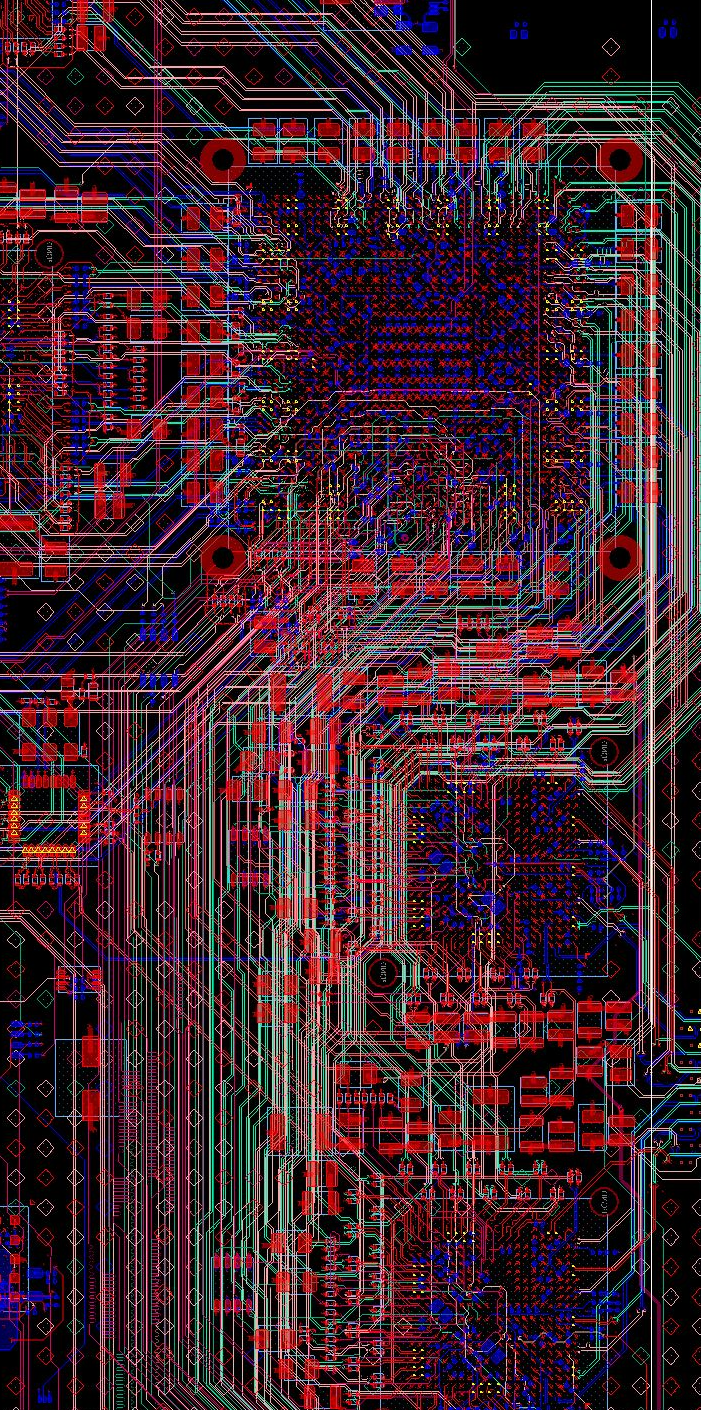
PCB layout is frequently not appreciated, but it is actually critical part of high speed logic, high speed interfaces, switch mode power supplies, analog front end, EMC both immunity and emmisions, environmental factors like corrosion, electromigration.
Areas we cover:
Rigid PCB from 1 to 64 layers
Flexi PCBs
HDI PCB
Fine Pitch BGA
Blind/Burried/Micro VIAs
High Speed
Signal Integrity
TDR Optimized
Characteristic Impedance Control
EMC Optimized
Microstrains Optimized Placement
Thermally Optimized
CAF Mitigation
Dendrite / Tin Whisker Mitigation
Clearance Creepage Control
Basic / Functional Isolation
Design for Manufacturability
Design for Testability
Our experienced PCB layout designers mastered art of tackling abovementioned and frequently seemingly contradicting rules.
We perform our layout on Cadence Allegro / Orcad and Altium Designer and KiCad.
We provide full pack of production documents (Gerbers, GBR 2x, ODB++, IPC-2581, 2D and 3D PDF for viewing, STEP file for mechanical engineers).
What differentiates us from competition for PCB Layout Design?
Our PCB layout designers are experienced eletronics enginers too. They understand circuitry and signals and concerns and apply mitigations accordingly.
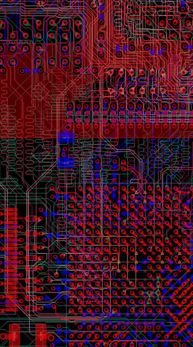
High speed: For high speed circuitry it is important to avoid sharp bends, keep matched lenghts, keep lines trully differential. We use well established tools to calculate characteristic impedance, dimensions, spacing. Each PCB materials have little bit different permittivity (even slighly changes with batch to batch variation) so we will ask your PCB material manufacturer about permittivity or recommended dimensions to achieve characteristic impedance as close as possible to desired value.
Where ESD diodes are populated on high speed interfaces, their capacitance (about 0.4pF for HDMI ESD diodes) disturbs locally characteristic impedance of interface, which can be seen on TDR measurement as depression. We compensate capacitance of ESD diodes with thinner trace in proximity of ESD diode so that characteristic impedance is constant.
Logic and analog: Capacitors for OpAmps and logic will be placed as close as possible to ICs. Extremly sensitive nodes like some OpAmp inputs will be guarded. Ground structure to separate sensitive circuitry from DCDC converters, relays, loads.
SMPS Crtitical loops and areas where high di/dt and dv//dt happen will be as small as possible. FB and COMP pins for DCDC controllers would be as far as possible noise-wise insulated from noisy node like switching node and bootstrap node. Current sense traces will be routed as Kelvin connection and high speed differential pair so regulator operates flawlessly.
Fragile components prone to cracking will not be placed in proximity of screws, depanelization tabs, connectors, push buttons, heavy components.
Environmental robustness. PCBs are designed to mitigate dendrites, electromigation, tin whiskers, CAF as much as possible.
Communication with circuitry designers. Some interfaces are designed with small margins for ground shift on PCB or between devices, we dont recommend such design, but we would discuss with customer.
Peer review.
Each PCB layout design is supervised electronic design engineer and concerns clarified with customer.
Our aim is to provide fit for purpose, robust, reliable, holistically designed electronis.
PCB layout is frequently not appreciated, but it is actually critical part of high speed logic, high speed interfaces, switch mode power supplies, analog front end, EMC both immunity and emmisions, environmental factors like corrosion, electromigration.
Areas we cover:
Rigid PCB from 1 to 64 layers
Flexi PCBs
HDI PCB
Fine Pitch BGA
Blind/Burried/Micro VIAs
High Speed
Signal Integrity
TDR Optimized
Characteristic Impedance Control
EMC Optimized
Microstrains Optimized Placement
Thermally Optimized
CAF Mitigation
Dendrite / Tin Whisker Mitigation
Clearance Creepage Control
Basic / Functional Isolation
Design for Manufacturability
Design for Testability
Our experienced PCB layout designers mastered art of tackling abovementioned and frequently seemingly contradicting rules.
We perform our layout on Cadence Allegro / Orcad and Altium Designer and KiCad.
We provide full pack of production documents (Gerbers, GBR 2x, ODB++, IPC-2581, 2D and 3D PDF for viewing, STEP file for mechanical engineers).
What differentiates us from competition for PCB Layout Design?
Our PCB layout designers are experienced eletronics enginers too. They understand circuitry and signals and concerns and apply mitigations accordingly.
High speed: For high speed circuitry it is important to avoid sharp bends, keep matched lenghts, keep lines trully differential. We use well established tools to calculate characteristic impedance, dimensions, spacing. Each PCB materials have little bit different permittivity (even slighly changes with batch to batch variation) so we will ask your PCB material manufacturer about permittivity or recommended dimensions to achieve characteristic impedance as close as possible to desired value.
Where ESD diodes are populated on high speed interfaces, their capacitance (about 0.4pF for HDMI ESD diodes) disturbs locally characteristic impedance of interface, which can be seen on TDR measurement as depression. We compensate capacitance of ESD diodes with thinner trace in proximity of ESD diode so that characteristic impedance is constant.
Logic and analog: Capacitors for OpAmps and logic will be placed as close as possible to ICs. Extremly sensitive nodes like some OpAmp inputs will be guarded. Ground structure to separate sensitive circuitry from DCDC converters, relays, loads.
SMPS Crtitical loops and areas where high di/dt and dv//dt happen will be as small as possible. FB and COMP pins for DCDC controllers would be as far as possible noise-wise insulated from noisy node like switching node and bootstrap node. Current sense traces will be routed as Kelvin connection and high speed differential pair so regulator operates flawlessly.
Fragile components prone to cracking will not be placed in proximity of screws, depanelization tabs, connectors, push buttons, heavy components.
Environmental robustness. PCBs are designed to mitigate dendrites, electromigation, tin whiskers, CAF as much as possible.
Communication with circuitry designers. Some interfaces are designed with small margins for ground shift on PCB or between devices, we dont recommend such design, but we would discuss with customer.
Peer review.
Each PCB layout design is supervised electronic design engineer and concerns clarified with customer.
Our aim is to provide fit for purpose, robust, reliable, holistically designed electronis.
Your Know How For Electronics LTD
2 Highlands Court, Cranmore Avenue, Solihull, England, B90 4LE
Company Registered for England & Wales Company No.11503324
Vat no: GB30403096
2 Highlands Court, Cranmore Avenue, Solihull, England, B90 4LE
Company Registered for England & Wales Company No.11503324
Vat no: GB30403096